In 2005, we published the work of transferring the ordered ulthathin AAO films onto other substrates (G. Q. Ding, et al., Fabrication of Controllable Free-standing Ultrathin Porous Alumina Membranes, Nanotechnology 16 (2005) 1285).
The present standard product: 50-80nm pore diameter, 100-110nm interpore distance, and 300-500 thickness.
Applications: As a mask for nanodot or quantum dot array by deposition methods. As a etching mask for nanopore array on substrates. Nanoimprinting template for nanostructures on softer surfaces, especially polymer surfaces.
Substrates: Successfully transferred onto silicon, silicon oxide, ITO, glass, copper, HOPG etc. The surface pretreatment of substrate is important. The customers can provide the substrates and finish the surface cleaning before substrate shipping.

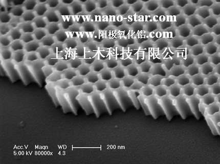
FESEM image of ultrathin AAO film on silicon substrate

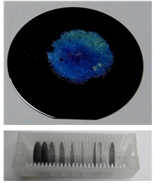
The digital photos of AAO films on 2 inch silicon wafer. The AAO sample area larger than 1cm2

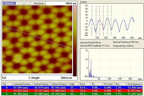
Typical 2D AFM image of free-standing AAO with ~45 nm nanopore arrays (AFM model: Veeco Dimensional Edge)
Application examples:

Silicon nanodot array. From the paper: G. Q. Ding, M. J. Zheng, W. L. Xu, W. Z. Shen, Fabrication of Nanocrystalline Si:H Nanodot Arrays with Controllable Porous Alumina Membranes, Thin Solid Films 508 (2006) 182.

Ge nanodot array. Image from:
Yourui Huangfu, Wenbo Zhan, Xia Hong, Xu Fang, Guqiao Ding and Hui Ye, Optimal growth of Ge-rich islands on Si (001) substrates with hexagonal packed pit patterns, Nanotechnology, 24 (2013) 035302.
Our advantages:
Ø Controllabe nanopore diameter
Ø Adjustable pore depth
Ø Highly ordered
Ø Transfer onto arbitrary substrates
Ø Very short lead time
We can design different ultrathin free-standing AAOs:
|
Nanopore diameter (nm)
|
Nanopore depth (nm)
|
Interpore distance (nm)
|
Barrier layer (BL) and aluminum base (AB)
|
Circular piece
|
Price ($)
|
|
3-10
|
50-400
|
20
|
Without BL and AB
|
>1×1cm2
|
150
|
|
10-20
|
50-400
|
25
|
Without BL and AB
|
>1×1cm2
|
150
|
|
20-30
|
100-400
|
50
|
Without BL and AB
|
>1×1cm2
|
150
|
|
30-50
|
100-400
|
70
|
Without BL and AB
|
>1×1cm2
|
150
|
|
40-90
|
100-400
|
100
|
Without BL and AB
|
>1×1cm2
|
150
|
|
* Remark: all these free-standing AAOs should be transferred onto substrates. The customer can provide specific substrates, and also can ask us to privide if we have.
|
References
1. Yourui Huangfu, Wenbo Zhan, Xia Hong, Xu Fang, Guqiao Ding and Hui Ye, Optimal growth of Ge-rich islands on Si (001) substrates with hexagonal packed pit patterns, Nanotechnology, 24 (2013) 035302.
2. Y. Y. Zhu, G. Q. Ding*, J. N. Ding, N. Y. Yuan, AFM、SEM and TEM Studies on Porous Anodic Alumina, Nanoscale Res. Lett. 5 (2010) 725-734.
3. G. Q. Ding, W. Z. Shen, M. J. Zheng, Z. B. Zhou, Indium Oxide “rods in dots” Nanostructures, Appl. Phys. Lett. 89 (2006) 063113.
4. G. Q. Ding, W. Z. Shen, M. J. Zheng, D. H. Fan, Synthesis of Ordered Large-scale ZnO Nanopore Arrays, Appl. Phys. Lett. 88 (2006) 103106. (Cited 41).
5. G. Q. Ding, W. Z. Shen, M. J. Zheng, Z. B. Zhou, Integration of Single-crystalline Nanocolumnars into Highly-ordered Nanopore arrays, Nanotechnology 17 (2006) 2590.
6. G. Q. Ding, M. J. Zheng, W. L. Xu, W. Z. Shen, Fabrication of Nanocrystalline Si:H Nanodot Arrays with Controllable Porous Alumina Membranes, Thin Solid Films 508 (2006) 182.
7. G. Q. Ding, M. J. Zheng, W. L. Xu, W. Z. Shen, Fabrication of Controllable Free-standing Ultrathin Porous Alumina Membranes, Nanotechnology 16 (2005) 1285. (Cited 56).
8. G. Q. Ding, W. Z. Shen, M. J. Zheng, W. L. Xu, Y. L. He, Q. X. Guo, Fabrication of Highly Ordered Nanocrystalline Si:H Nanodots for the Application of Nanodevice Arrays, J. Cryst. Growth 283 (2005) 339.
9. W. L. Xu, M. J. Zheng, G. Q. Ding, W. Z. Shen, Fabrication and Optical Properties of Highly Ordered ZnO Nanodot Arrays, Chem. Phys. Lett. 411 (2005) 37. (Cited 33).